The University of Notre Dame has accepted delivery of a high-end Vistec EBPG 5200 electron-beam lithography system to campus. The multi-million dollar tool, purchased from Vistec Lithography Inc., will be installed in the Notre Dame Nanofabrication Facility (NDNF) in the new Stinson-Remick Hall of Engineering. The equipment was purchased with the University’s Strategic Research Initiative funding.
“The addition of Vistec’s powerful electron-beam lithography system to our existing equipment portfolio will enable our nanofabrication facility to support the leading-edge of device research for years to come,” said Patrick Fay, professor of electrical engineering at Notre Dame and NDNF director.
The EBPG 5200 is the latest version of Vistec’s highly successful and field-proven EBPG electron-beam lithography tool series. The EBPG 5200 at Notre Dame features 50 and 100kV accelerating voltage, is equipped with a 50 MHz, 20-bit pattern generator, with large field size operation, and the ability to write full 200 mm wafers.
The Vistec EBPG 5200 routinely generates structures less than 8 mm on varying substrate sizes from piece parts of a few millimeters to full patterning across a 200 mm diameter wafer. The system incorporates an interactive graphical user interface (GUI) that provides ease of use for diverse, multi-user environments. Vistec’s high-current column design minimizes exposure time for complex nano-patterning.
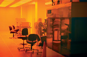
The NDNF is a world-class, 9,000-square-foot teaching and research cleanroom. The facility provides a comprehensive suite of state-of-the-art equipment for designing and manufacturing integrated circuits and devices with geometries of a few nanometers.
NDNF researchers—which include internal and external academic and corporate clients—use the facility to explore a wide range of materials and processes, including silicon-related electronic devices, compound semiconductors, zinc selenide nanowires, carbon nanotubes, graphene, and organic polymer-based materials. In addition, the NDNF facilitates the study of microfluidic technologies for medical applications and micron-scale mechanical device fabrication.
The NDNF consists of three large areas: a class 10,000 area that houses equipment for chemical-mechanical polishing, wafer thinning, packaging and assembly, and molecular beam epitaxy; and class 1,000 and 100 areas that contain capabilities for metal deposition, lithography, oxidation, dielectric deposition, plasma processing, and wet-chemical processing.
The Vistec EBPG 5200 will occupy a dedicated space in the NDNF’s class 100 area.
In the 1980s, Notre Dame was one of the first universities to focus strongly on nanoelectronics. The university’s Center for Nano Science and Technology (NDnano), established in 1999, continues to explore the fundamental concepts of nanoscience to develop unique engineering applications using nano principles. The center is composed of a multidisciplinary team of researchers from various science and engineering fields. The invention of Quantum-Dot Cellular Automata (QCA) and the establishment of the Midwest Institute for Nanoelectronics Discovery (MIND) are among NDnano’s notable accomplishments.
Contact: Robert M. Dunn, 574-631-9854, rdunn@nd.edu
Originally published by at newsinfo.nd.edu on September 21, 2011.